Development of custom electronic boards with CNC Router.
Features
For voltage, resistance and continuity tests, we use the Fluke brand multimeter. It is a piece of equipment of excellent quality and highly recommended for its precision and reliability.
Main features
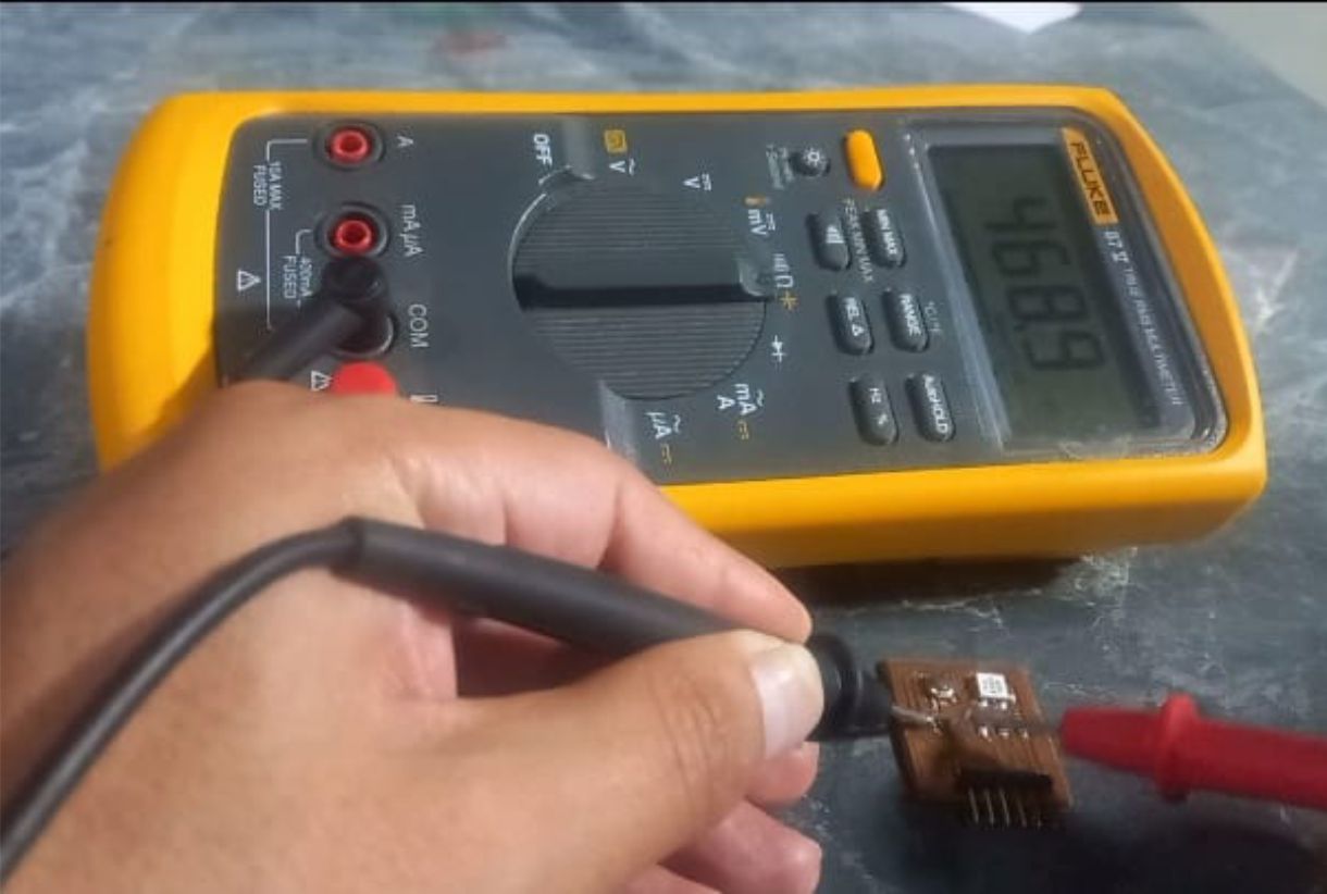
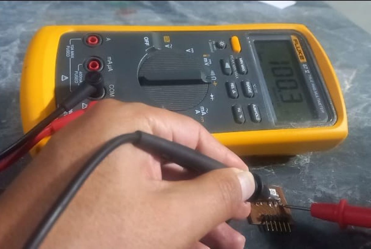
For the first tests with the multimeter, we use the TDS sensor as input, which measures water quality. I proceeded to connect the clamps, I connected the retractable to the signal input and the alligator to GND.
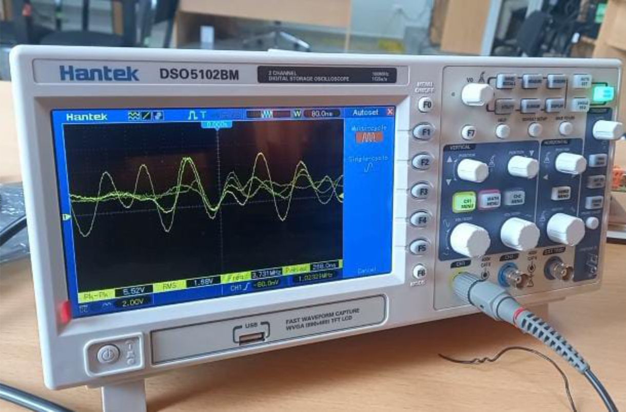
Yes, square wave type signals can be displayed to take values from the machine and ensure that measurements are correct. In addition, the distorted sine wave type signal from the TDS sensor can be observed to evaluate its behavior and accuracy.
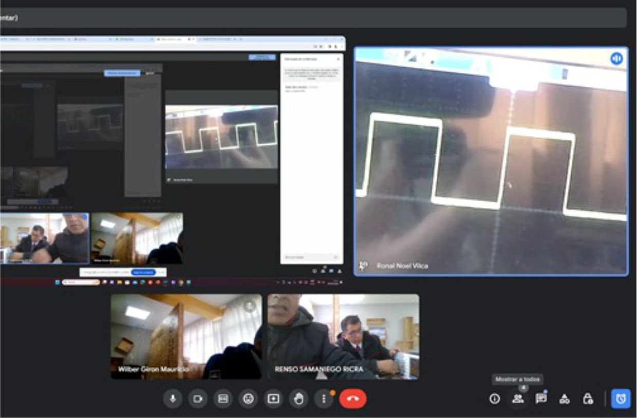
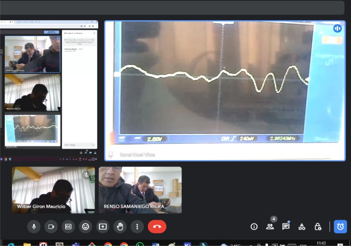
During the discussion with my colleagues, we analyzed the values displayed by the oscilloscope. We use channel 1 and perform automatic calibration to obtain the values and ranges of our sensor. In my case, we observed that the maximum values reached 560mV. To record this data, we clicked on snapshot screenshot

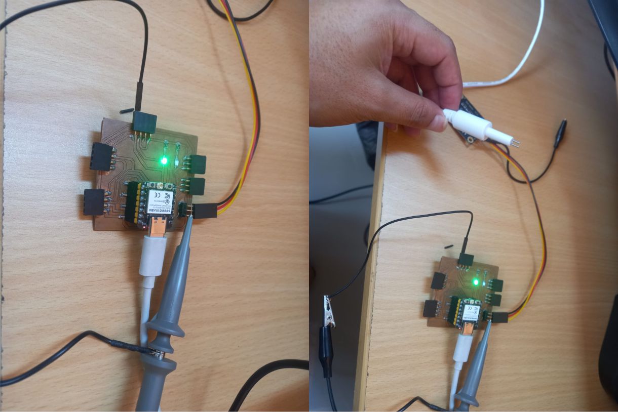
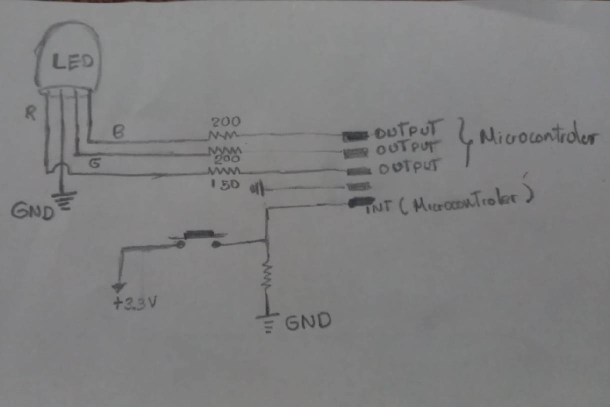
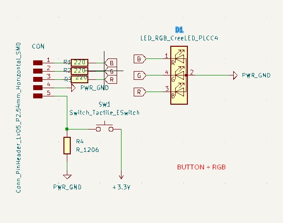
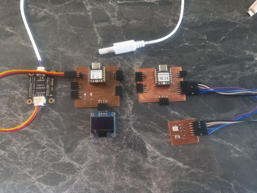
To perform measurements, such as resistance, voltage, and continuity testing, we use the test board we developed. In my case, I used an additional extension board that has a push button as input and an RGB LED as output.
As can be seen in the image, we measure the resistors that we will connect to the anodes of the RGB LED. We use two 150 ohm resistors for colors G and B, and one 100 ohm resistor for color R. We also use a 470 ohm resistor for the push button.
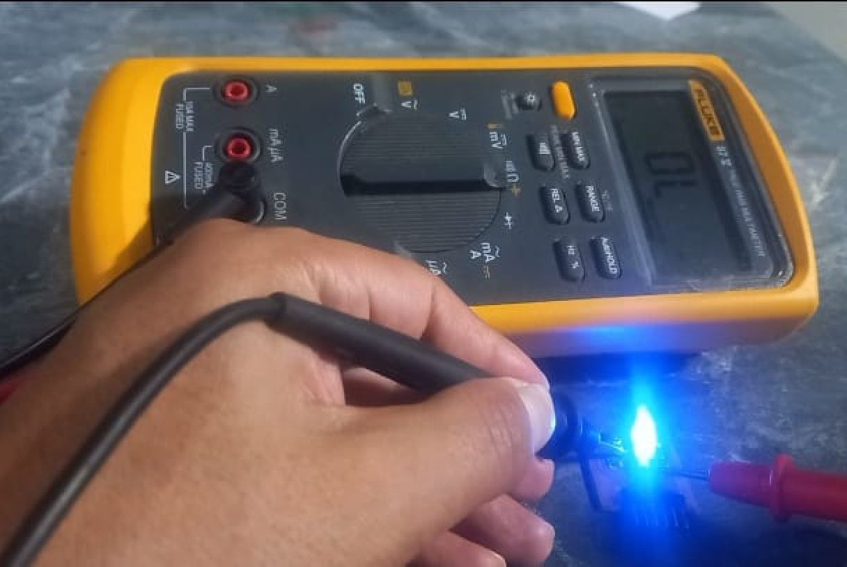
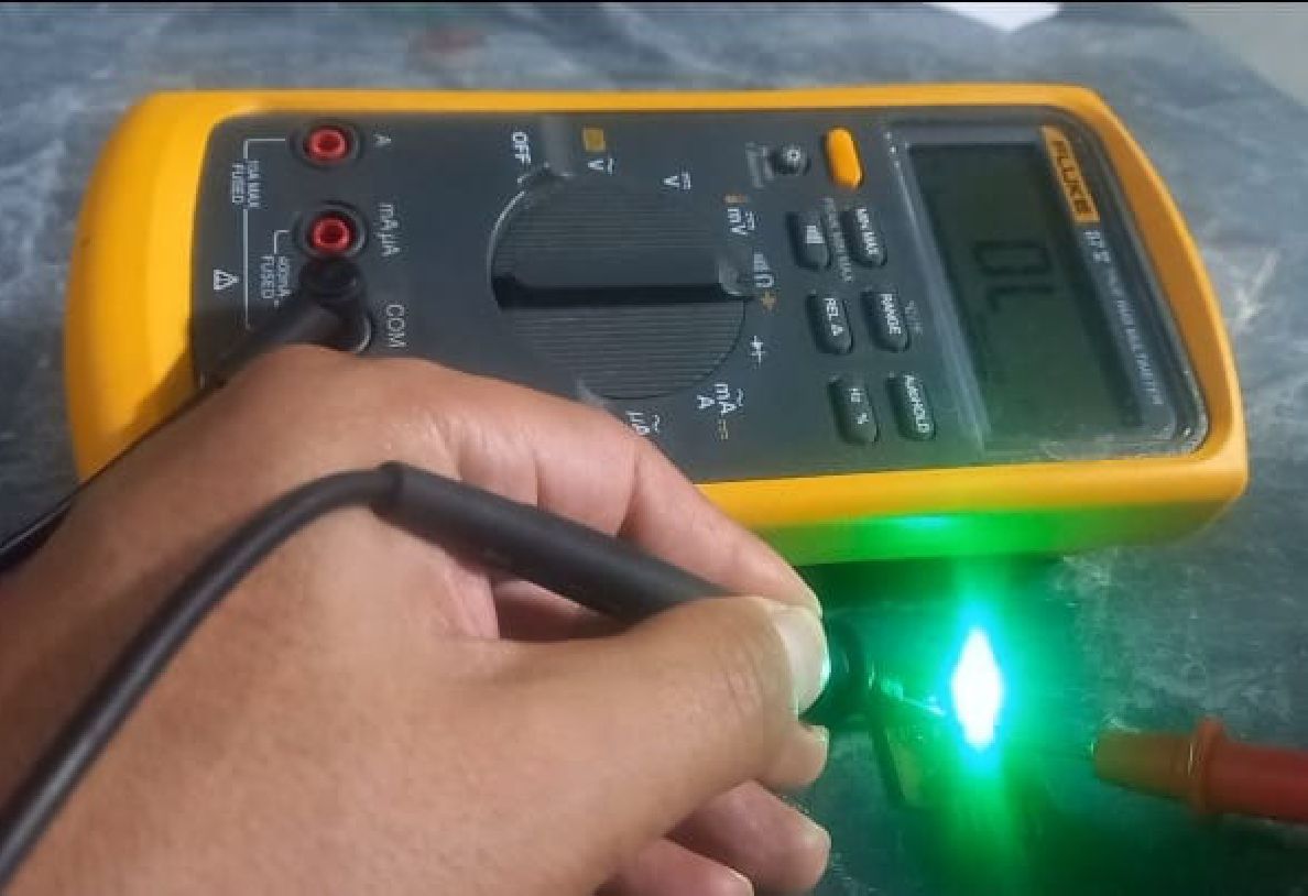
We also carry out a test to verify if the RGB LED is operational. To do this, we perform a diode test. We place the black clamp on the cathode and the red clamp on the anode of the LED, as can be seen in the video.

We learned that it is crucial to perform a calibration using the equipment's own output values or signals of the oscilloscope. Our initial mistake was not understanding why the sensor values were so high and seemed wrong. However, by realizing the importance of testing with the equipment's own output first, we were able to obtain more precise and realistic values. This experience taught us a valuable lesson, and each week we continue to learn and improve.
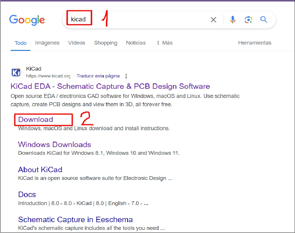
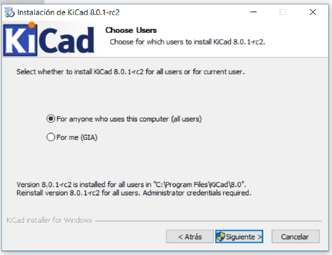
I will use KiCad software. Before starting, I will proceed with downloading and installing the program.
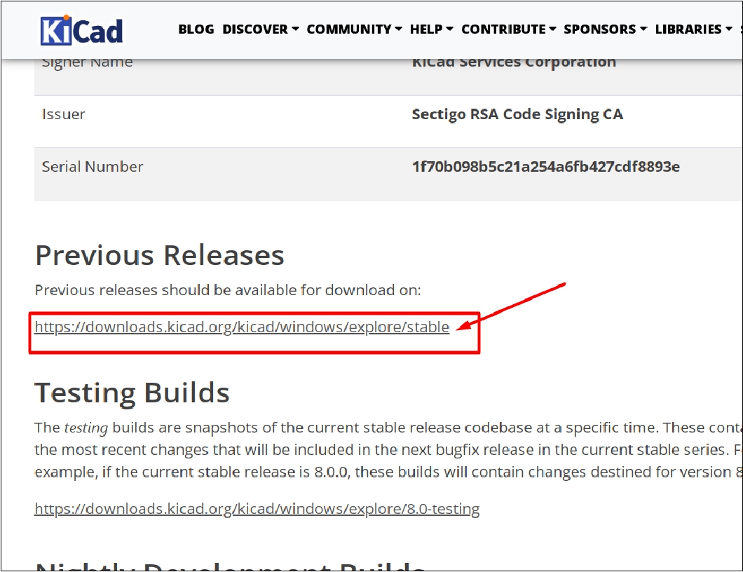
To get started, open your browser and search for 'KiCad' on Google. Then, click on the Downloads section. A window will open where you can select your operating system.
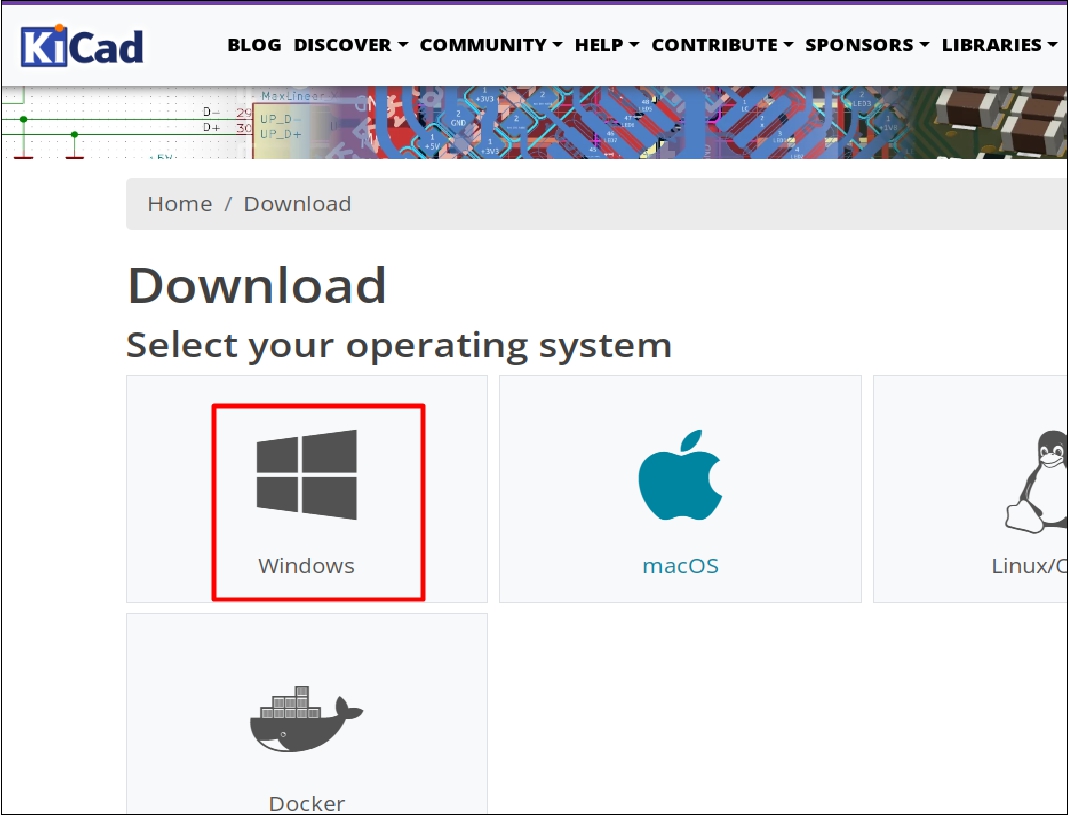
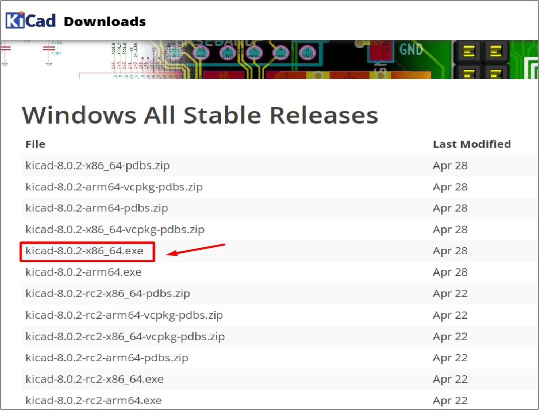
Once you have selected your operating system, click on the stable link that will take you to the download options. In this section, choose your computer's operating system; for example, in my case it is Windows 64. Click on the corresponding option and the download will start automatically.
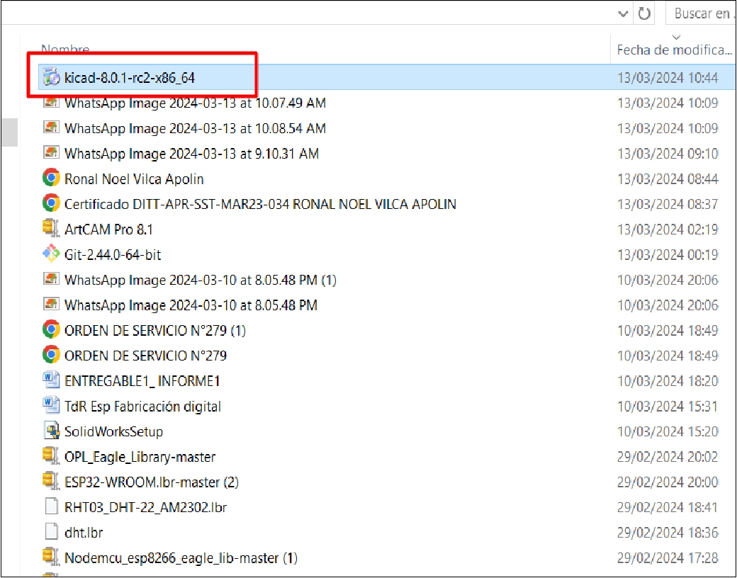
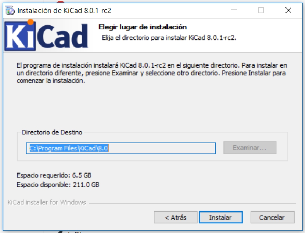
Once the download is complete, the next step is to double-click on the downloaded file named KiCad 8.0.1 and then click 'Next' to start the installation process.
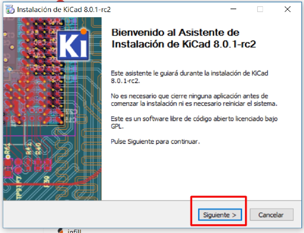
The installation process is to keep clicking 'Next' at each step until the installation is complete.

The KiCad software has been installed and is ready for first use. In this case, an RGB control module and a configuration button with a pull-up resistor will be developed, which will be detailed later.
This week I will be working on designing and building a small input and output board. As input, I will use a push-button with a pull-up type configuration, and as output, I will implement an RGB LED for control, both integrated on a single board.
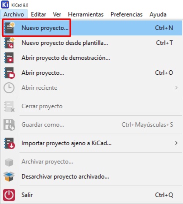
To begin the design, the first step is to create a folder where all the work will be stored. Once this is completed, we proceed to open the work environment and, in the toolbar, select the "FILE" section and then "New project".
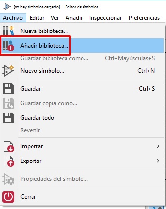
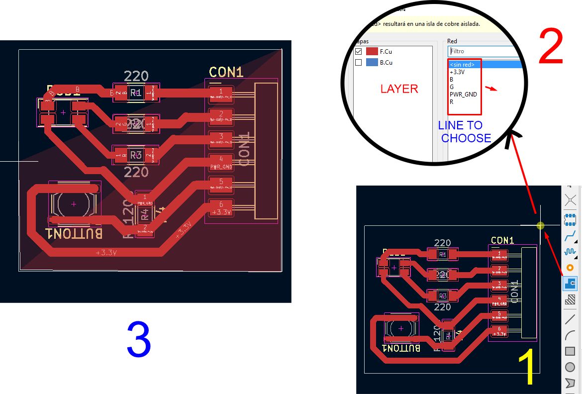
Correct. Once in the work environment, continue to the toolbar and select "FILE", then "Add Library". This will allow me to add the necessary libraries to the design project
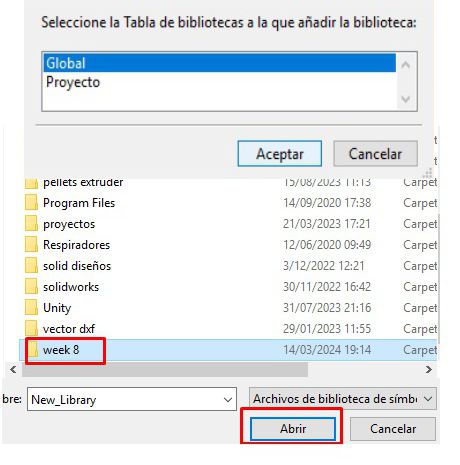
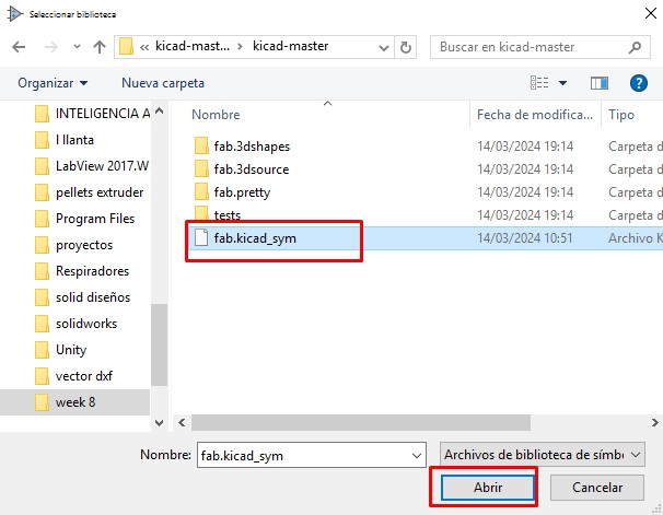
You will then be asked to choose between "Global" or "Project." In this case, select "Global." Then, proceed to choose the “Fab.Kicad-sigm” library.
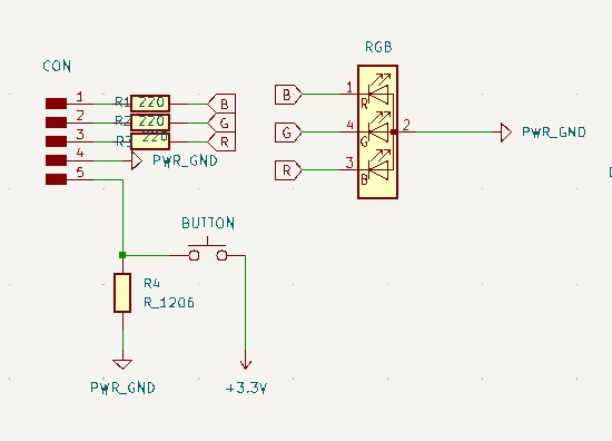
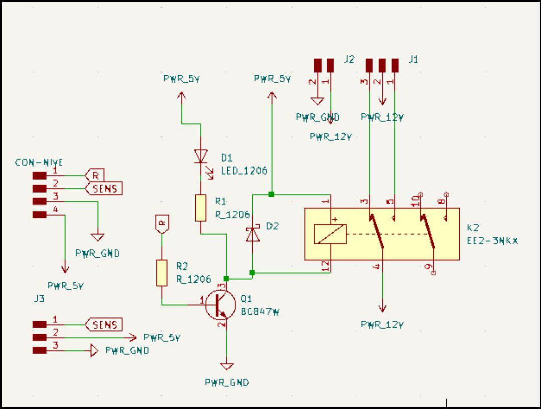
Well, let's get to work! We will begin development in the schematic environment and incorporate all the necessary components for your electronic board.
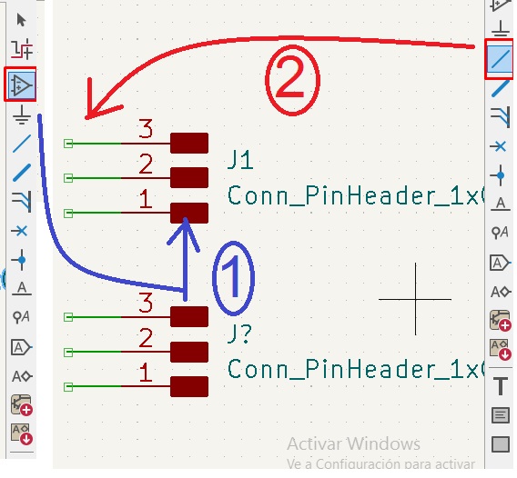
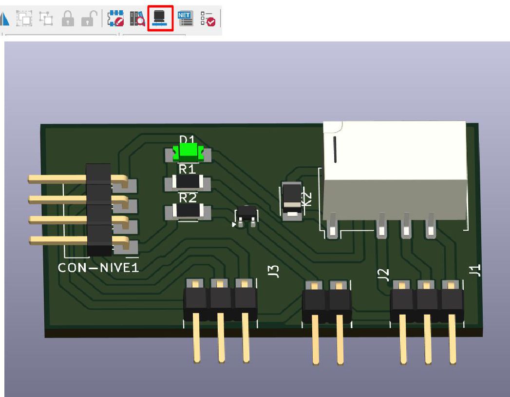
Once all the components are in place, it is time to proceed with routing the board. To do this, we switch to the plate editor. It is crucial to correctly arrange the connections to avoid errors.
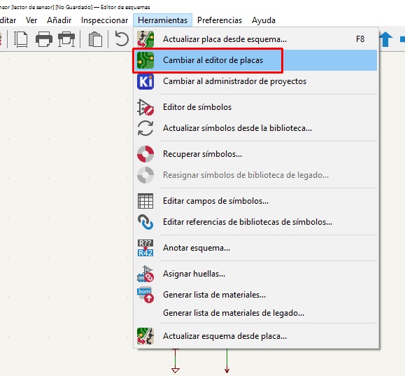
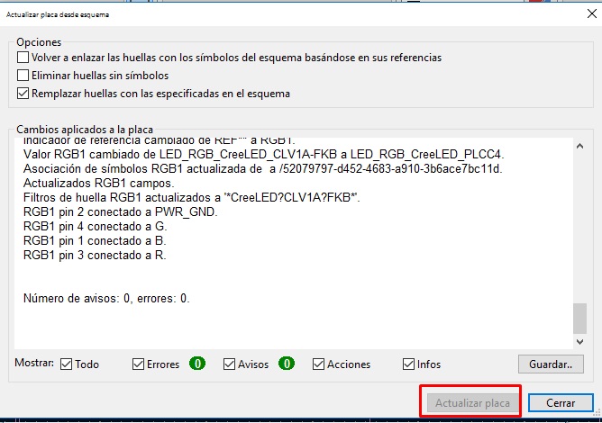
Once in the board routing environment, the next step is to update the board from the schematic environment. When you do this, a window will appear indicating that the components are being extracted. Then, simply click 'Update'.
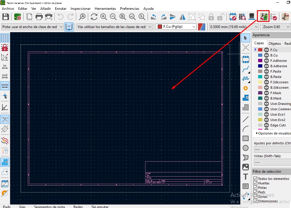
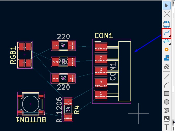
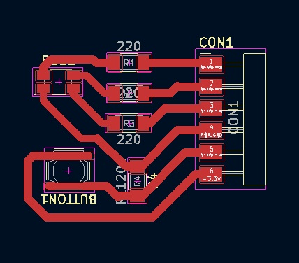
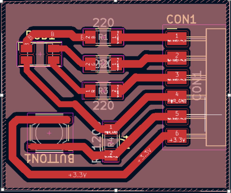
As we can see, all the components have been inserted correctly. Now we proceed to routing, where we will join the components according to the design in the schematic. It is important to note that when selecting, the software will only indicate the direction to follow. Additionally, it is essential to understand that the recommended tracks for small SMD boards range between 0.4 and 1mm wide.
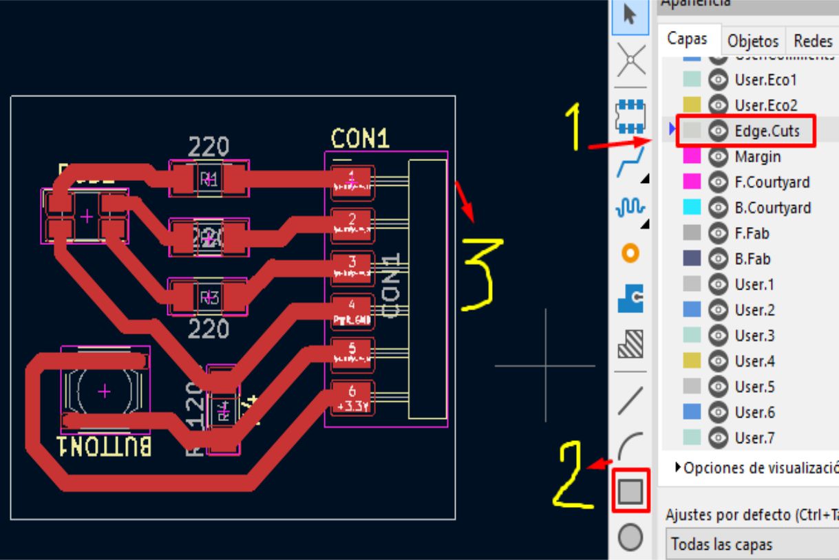
The next step is to delimit the size of the electronic board by creating an outline. To do this, we select "Edge Cuts". It is crucial to carry out this step, as it allows us to define the exact size of the plate, which makes it easier to perform other operations. Once selected, we proceed to define the dimensions
Then, right click on one of the corners and a window will appear asking you to choose which face the fill will be made on. Upon confirming the selection, click "OK" and you will have completed the process.
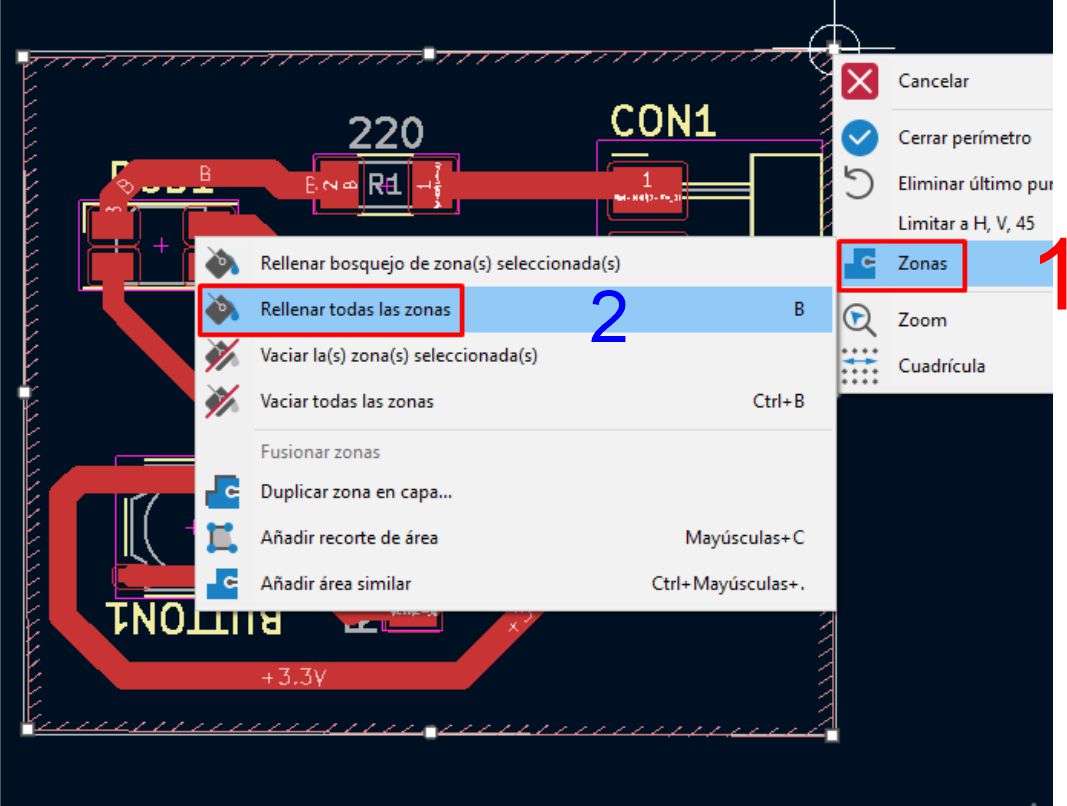
Then, click on a corner and a small window will appear. In it, select "Zones" and then "Fill all zones."
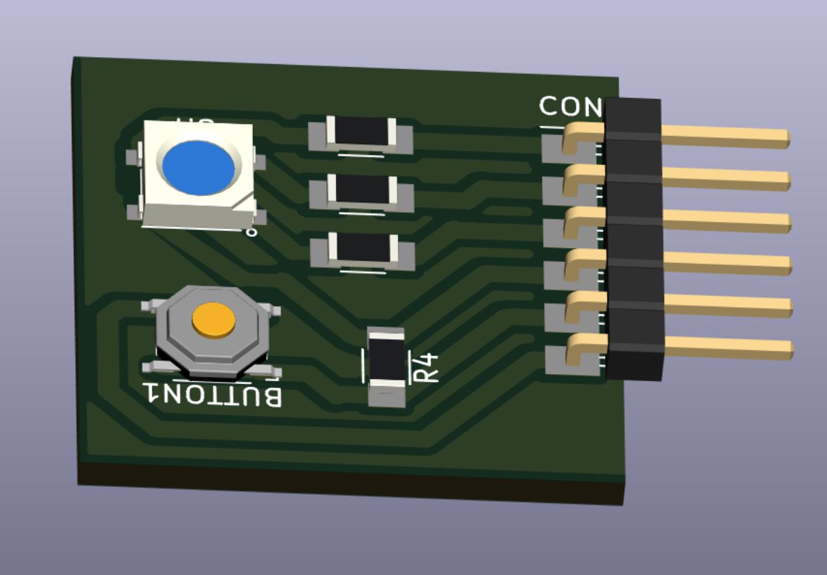
Finally, we request a 3D visualization of the electronic board, and that's it! That's all.
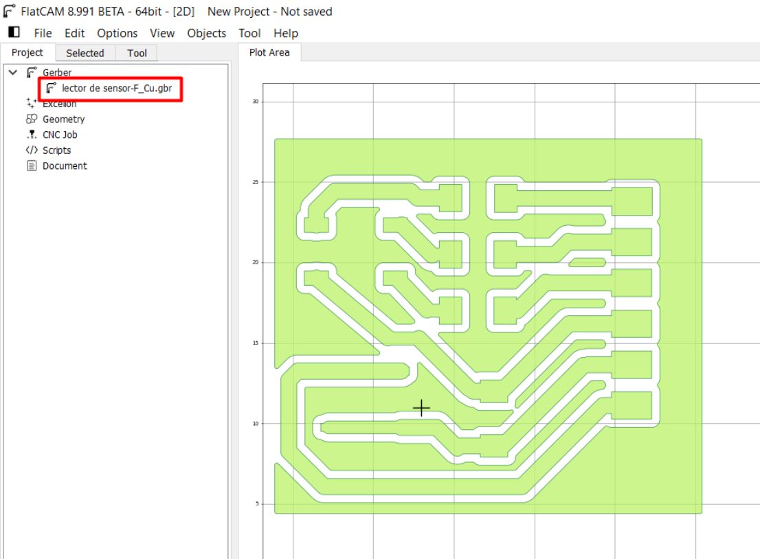
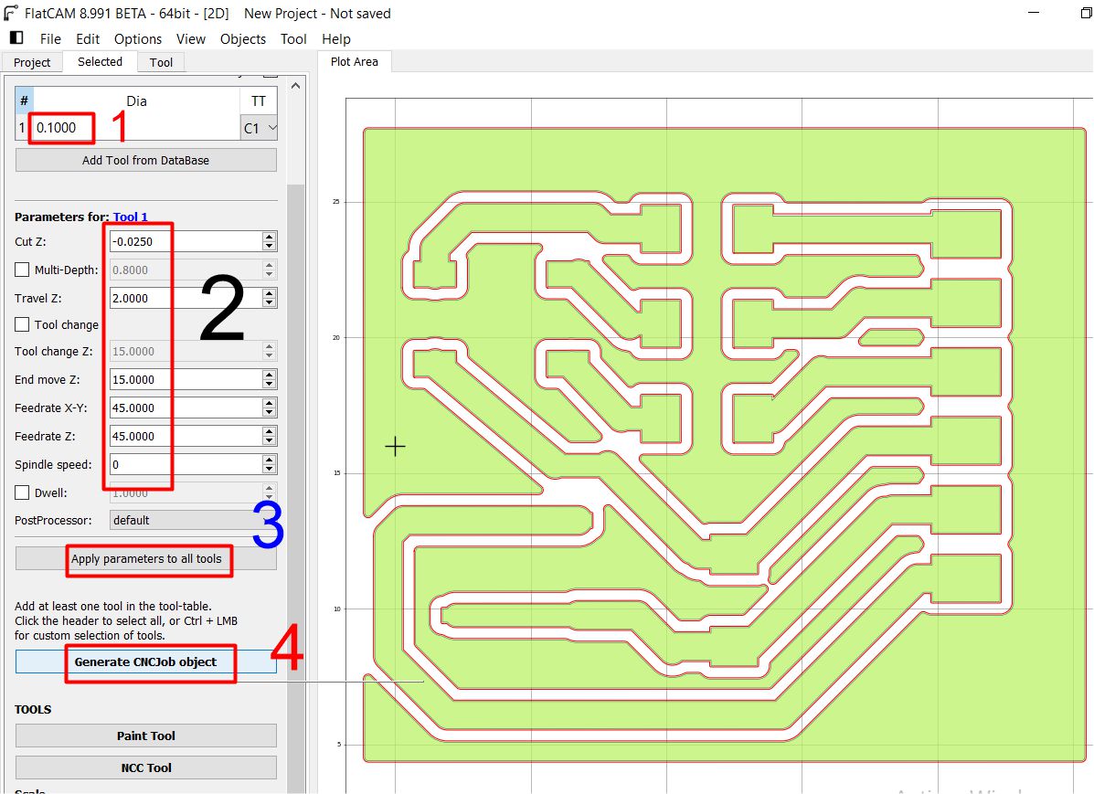
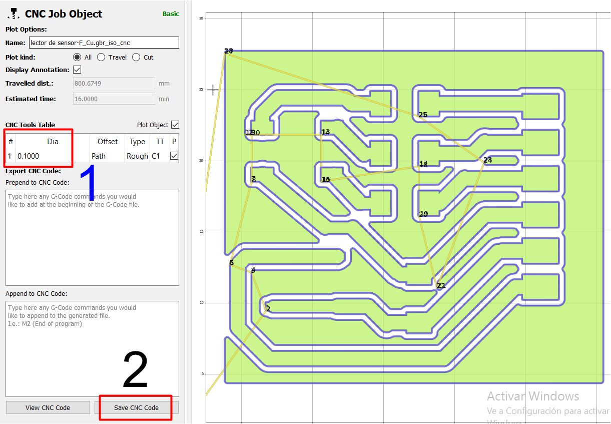
After completing the design, we open the Flatcam software and import the corresponding Gerber file. Next, we set up the milling tool, in my case using a 30 degree lance tool with a diameter of 0.1 mm and tool code 3.175. Subsequently, we establish the roughing depth of the copper, in my case I set it to 0.0250, with a feed speed in the X, Y and Z axes of 45 p/min and a movement speed in the Z axis of 15 p/min . Finally, we generate the milling path.
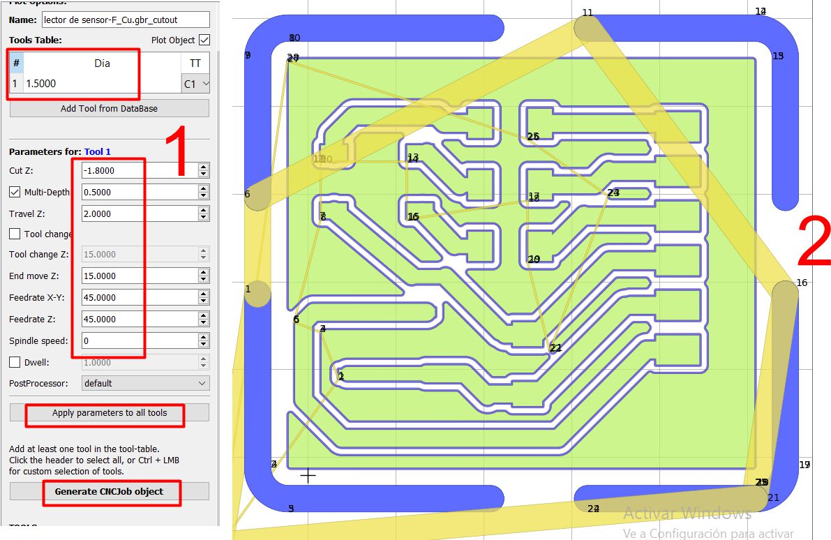
As you can see, the routing of the tracks has been completed successfully. Now, the next step is to generate the outer cut. To do this, we will change the tool to a 1.5 millimeter diameter, four-flute milling cutter. The cut will be made at a depth of 1.8 mm.
In the following videos, you will see the track routing process and the exterior cutting process.
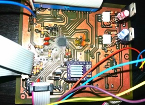
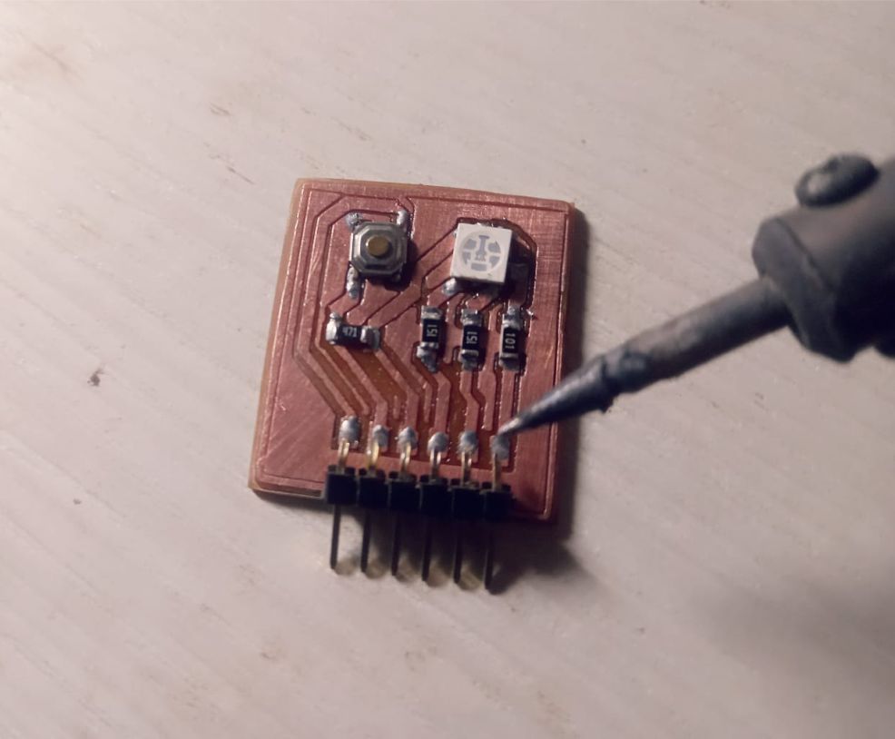
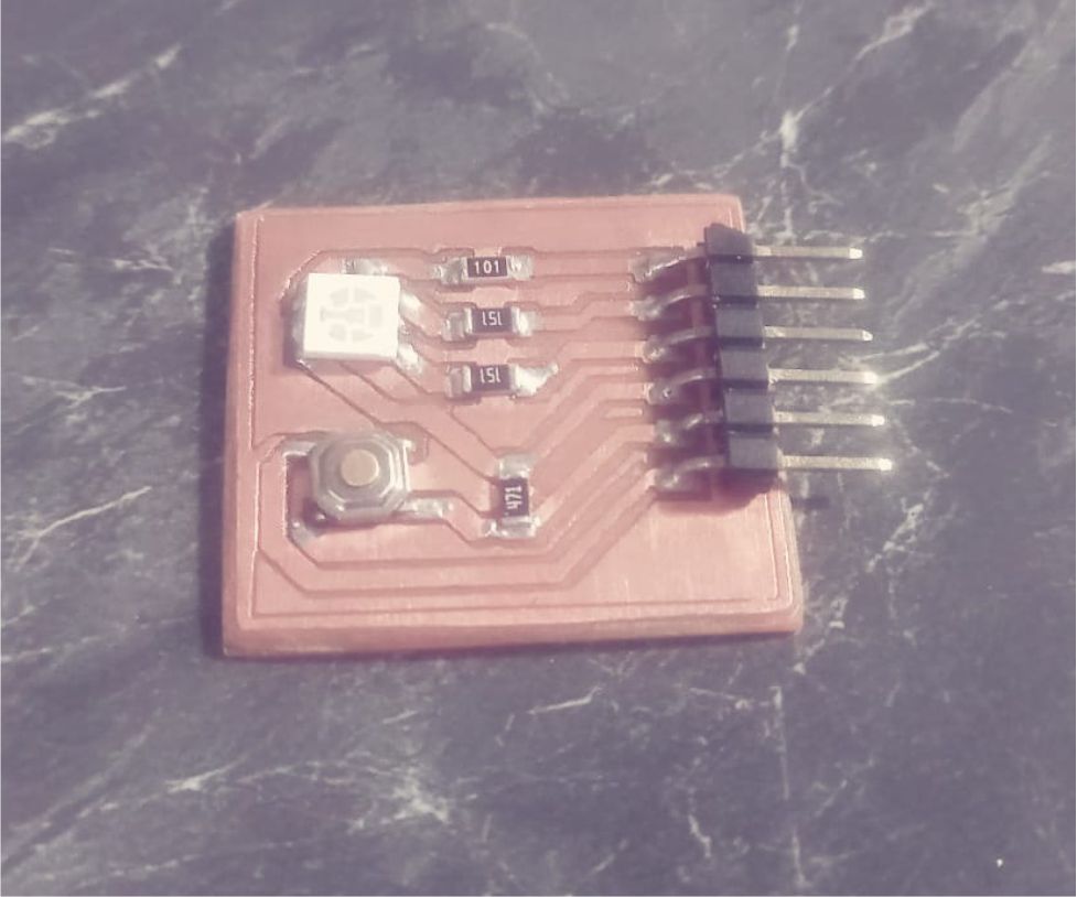
In the following images, you can see the finished plate, which has approximately dimensions of 2.5 x 2.7 cm. Now, we prepare to solder all the necessary components.
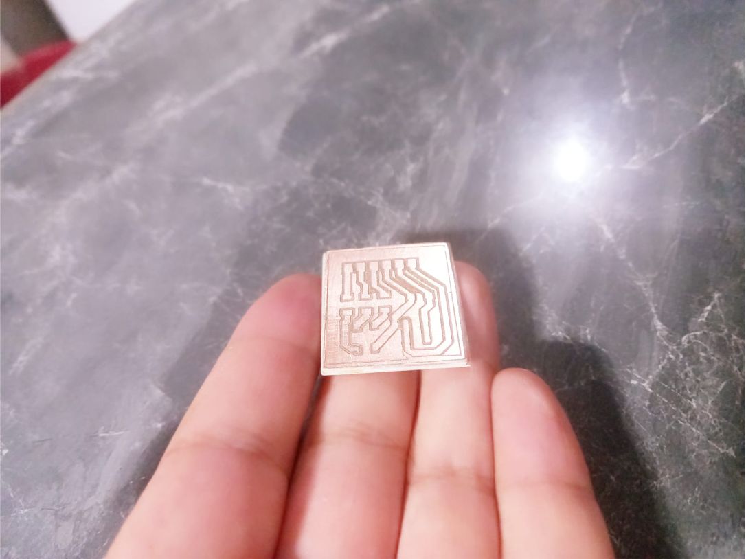
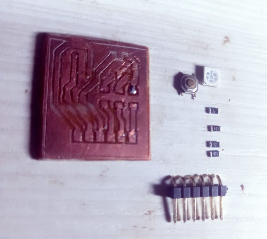
The components necessary to use are the following: a motherboard, a button, an RGB LED, a 100 ohm resistor, a 470 ohm resistor, two 150 ohm resistors and a 1x6-pin connector
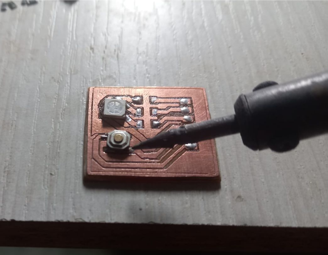
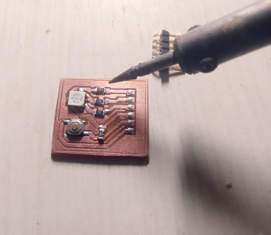
The next step is to solder all the components, following the established plan. The image shows how each component has been arranged, exactly matching the previous design.
It was developed for implementation in my final project
Once the soldering is completed, the next step is to test the operation of the board. To do this, we will need the motherboard developed previously to carry out the necessary tests.
The video shows the operation of the board. In this case, it was programmed so that when you press a button as input, the response is a set of RGB lights. This is just an example of the programming carried out; It is possible to create multiple arrangements and functionalities.
This week has been incredible for me. I used to use EAGLE software for my electronic board designs, which I thought was excellent. However, it had an important limitation: it did not allow viewing in 3D. Instead, I recently learned how to use the KiCad software, which is fantastic. Not only is it easy to use for design, but it also offers the ability to visualize both components and parts in 3D. Also, best of all, it is open source software. Without a doubt, I will recommend it to my colleagues in Huánuco and to anyone interested in electronic board design.
1. RGB schematic.sch
1. RGB schematic.pcb
1. RGB schematic.grb
Development of custom electronic boards with CNC Router.

Development of personalized keychains and ornaments with CNC Laser.
Development of custom machines "Desktop CNC Laser.

Huánuco is a Peruvian city, capital of the district, province and department of the same name in the north-central area of the country. The city has a population of 235,529 inhabitants. .